FPGA Frequency Measurement and Acoustic Event Classification
System-Level Design, SSIs M.Sc. (USN/BME) · Autumn 2025 · Academic project
A hierarchical VHDL system that measures an input signal's frequency and classifies acoustic events into bands, verified in ModelSim and synthesized on an Altera Cyclone III with full timing closure.
- VHDL
- FPGA
- ModelSim
- Quartus
- TimeQuest
- RTL design
Overview
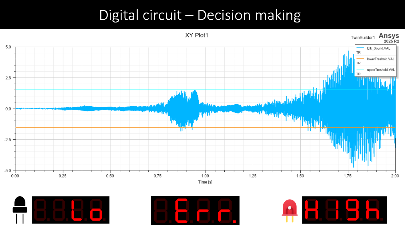
The digital back-end of a wildlife acoustic sensor node concept: measure the dominant frequency of an incoming signal and decide, in real time, whether it falls into one of several frequency bands of interest. The design is fully synchronous, parameterized with VHDL generics, and was taken through the complete flow from testbench simulation to synthesis, static timing analysis, and an on-hardware demo.
My contribution
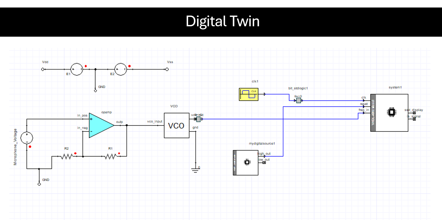
I designed and implemented the digital back-end: the frequency-measurement cores, the band detectors, the display decoders, and their testbenches. The wider design-lab project (MEMS microphone model, analog front-end, system digital twin) is described in the System-Level Sensor Node project.
Technical approach
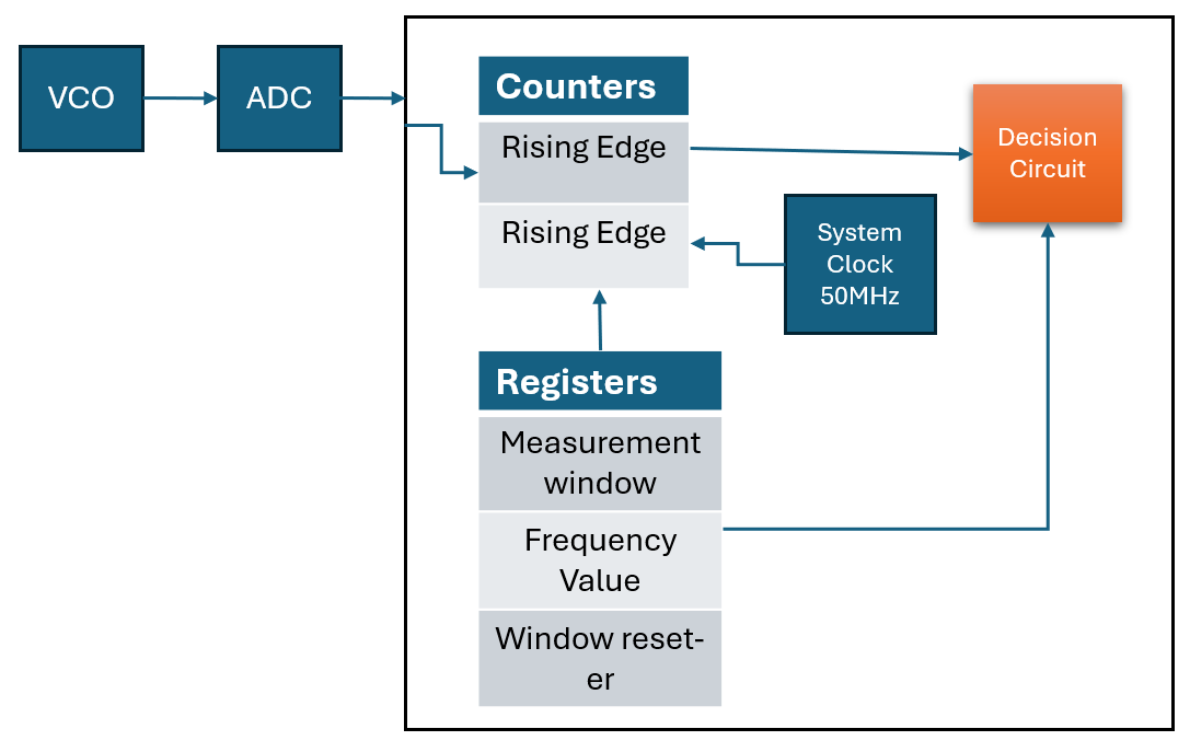
- Window-based frequency counter with generics for measurement resolution and system clock frequency, plus a second period-based counter for instantaneous measurement
- Two-stage input synchronizer with registered edge detection to safely sample the asynchronous input
- Three band-specific frequency-range detectors instantiated from one generic entity, each with activity and gap counters so a classification asserts only after sustained in-band activity and tolerates brief dropouts
- Seven-segment display decoders for live readout
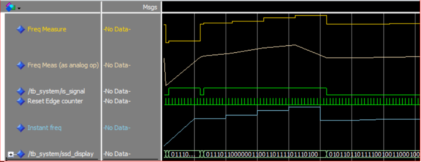
- Module- and system-level ModelSim testbenches, including a scripted 15-step frequency sweep around the decision threshold
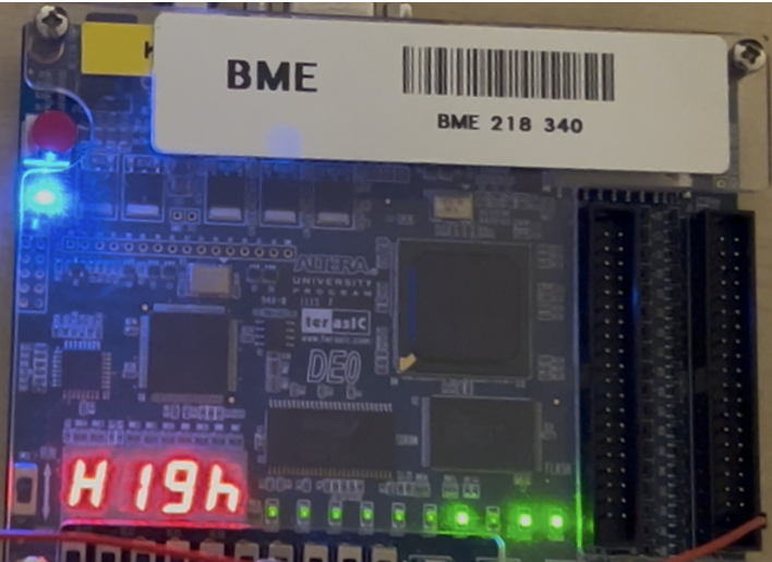
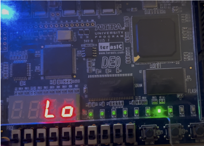
- Synthesis and TimeQuest static timing analysis in Quartus II 13.1, then a hardware demonstration on the FPGA board
Results
- Met timing on an Altera Cyclone III (EP3C16F484C6) at the 50 MHz clock constraint with worst-case Fmax of 161.6 MHz and zero total negative slack
- Compact implementation: 177 of 15,408 logic elements and 119 registers
- Demonstrated live on hardware with a signal generator, alongside ModelSim and Ansys Twin Builder co-simulation results
Media