Optical Profilometry of RF MEMS Structures
Department of Microsystems, USN · Norway · 2024/2025 · Academic project · Group of 4
White-light interferometric metrology of RF MEMS switch structures with a Veeco Wyko NT9100, resolving sub-nanometer surface roughness.
- Interferometry
- Metrology
- RF MEMS
- Surface roughness
Overview
Dimensional and roughness metrology of provided RF MEMS switch structures using phase-shifting and vertical-scanning interferometry, benchmarked against optical microscopy.
Technical approach
- Veeco Wyko NT9100 optical profilometer in PSI mode for smooth surfaces and VSI mode for taller steps
- Stitched full-sample topography plus local roughness maps
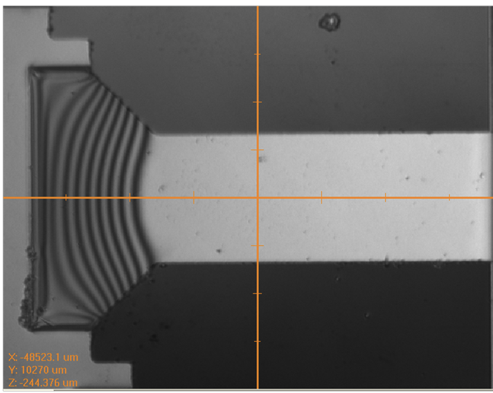
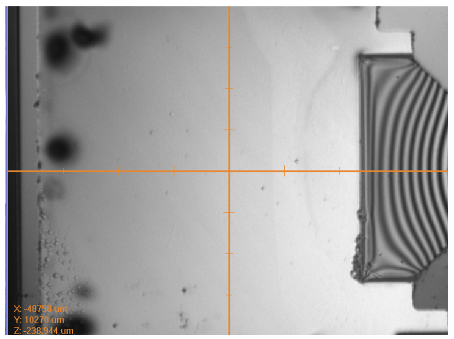
- Cross-checked lateral dimensions against calibrated optical microscopy
Results
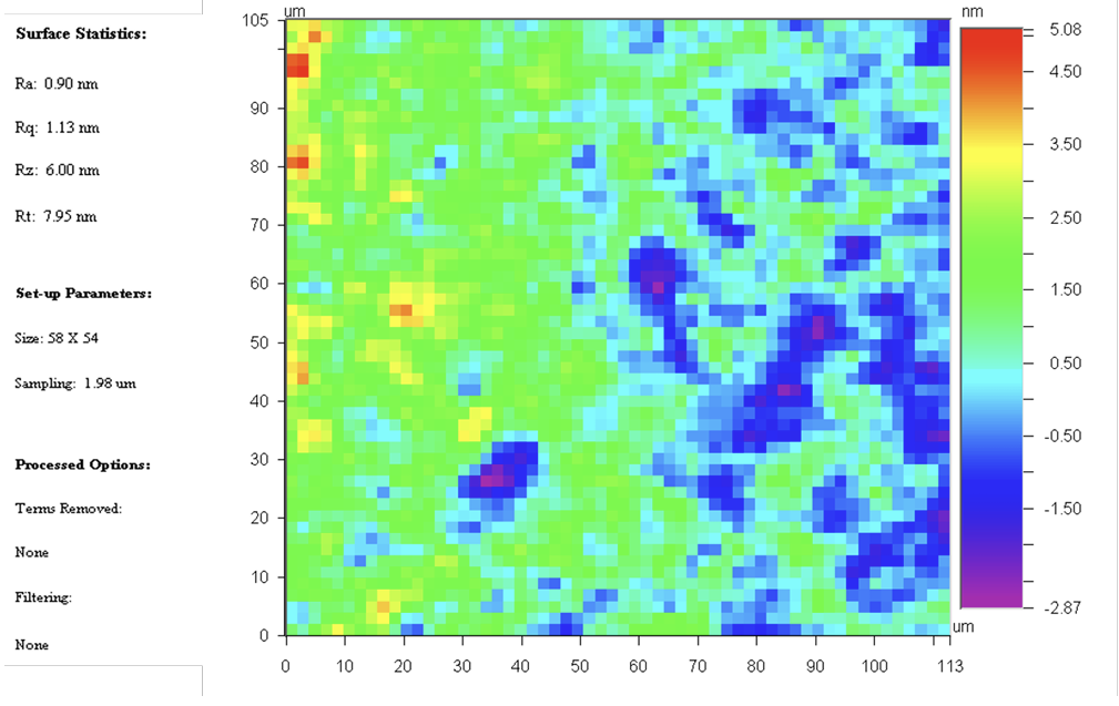
- Measured 0.42 nm surface roughness on gold transmission lines (PSI), 0.9 nm on the switch bridge, and 6.2 nm on the silicon substrate
- Extracted feature dimensions and step heights across the structures
Media