Cleanroom Microfabrication of Silicon Microstructures
Department of Microsystems, USN · Norway · Spring 2025 · Academic project · Group of 5
A complete microfabrication flow on silicon wafers in the USN cleanroom: oxidation, photolithography, dry and wet etching, and metallization, with metrology at every step.
- Cleanroom
- Photolithography
- ICP-RIE
- KOH etching
- Thin films
- Metrology
Overview
Three 4-inch silicon wafers taken through a full process flow, with each step verified by measurement rather than assumed. The companion design exercise specified a process-integration plan for an AlN MEMS microphone (not fabricated).
The accompanying literature reviews from this course fed into two published books (team contributions): the photoresist processing techniques chapter in Photoresist Technology in Microsystems (Springer, 2025) and content in Green Etching Techniques for MEMS Applications (CRC Press, 2025).
Technical approach
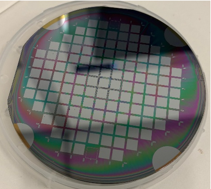
- Dry thermal oxidation at 1100 C targeting a 200 nm oxide
- Spin-coated AZ 4562 photoresist, proximity UV exposure, and TMAH development
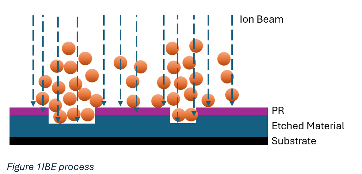
- ICP-RIE dry etching of SiO2 with CHF3 and Ar chemistry, followed by O2 plasma ashing
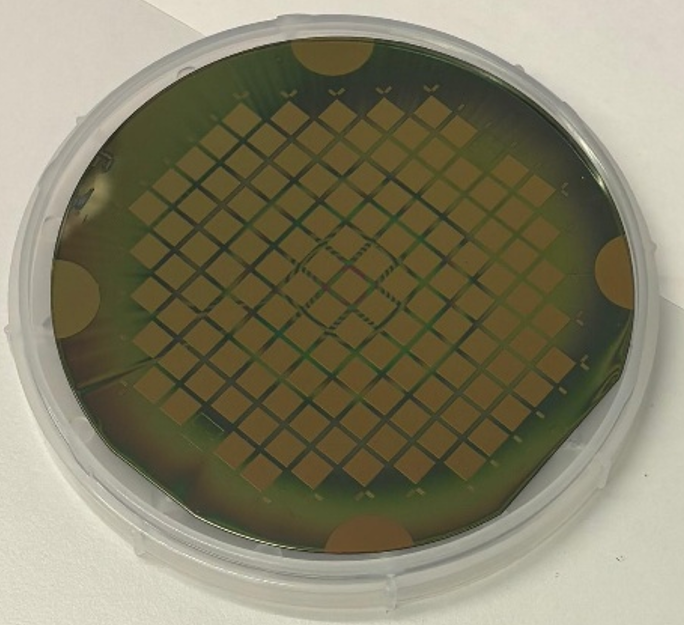
- Anisotropic KOH wet etching (10 percent, 70 C)
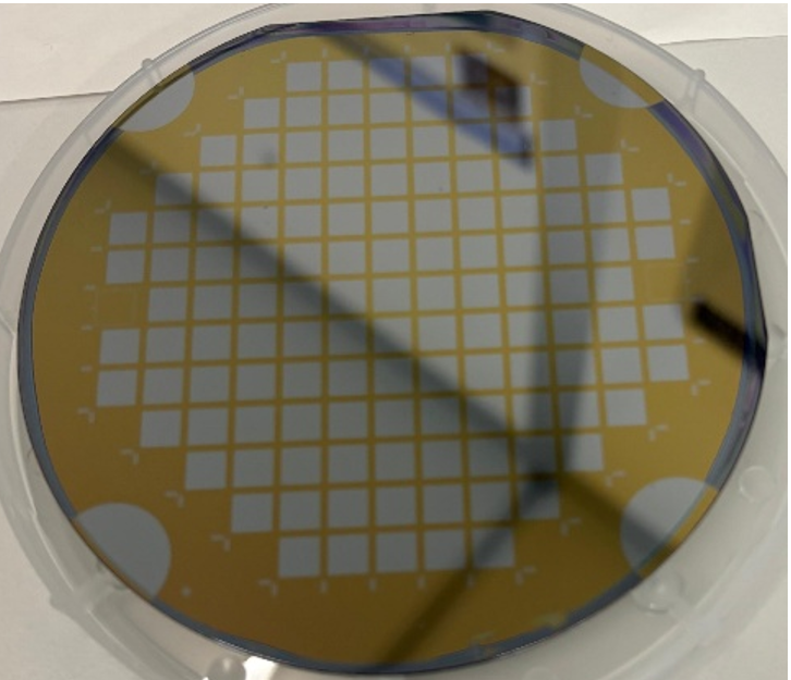
- Thermal evaporation of an Al then Cu bilayer without breaking vacuum, thickness-controlled by quartz crystal microbalance
- Stylus profilometry (Dektak 150) and spectroscopic ellipsometry after each relevant step
Results
- Grown oxide measured at 234 to 253 nm across wafers by ellipsometry
- KOH etch depths of about 18.8 um after 23 minutes and 73.9 um after 80 minutes
- Deposited metal stack measured at about 247 nm Al plus 712 nm Cu
Constraints and lessons
The process-integration design for the AlN microphone (sputtering, chlorine-based metal etch, PECVD standoffs, eutectic bonding, backside DRIE) stayed on paper; documenting the difference between a designed process and an executed one was part of the point.
Media